

Declarare adaos comercial practicat la ANAF – baza legala Fimele cu activitate de comert/ prestari servicii/ productie au obligatia declararii la ANAF a adaosului comercial practicat/ comision. Baza legala: Legea 12/1990 privind protejarea populatiei impotriva unor activitati de productie, comert

INFOGRAFIC: Infiintari firme – ce este sediul social? Sediul social poate fi tradus prin „domiciliul firmei” tale. Este o adresa, unde poti fie sa iti desfasori activitatile, fie sa ramana doar o adresa de corespondenta pentru institutiile statului, care pot

TVA la incasare- ce inseamna si cand se aplica? TVA la incasare este un sistem care permite amanarea platii, respectiv a deducerii TVA pana la data incasarii facturilor emise catre clienti si platii furnizorilor. Ce inseamna efectiv in relatiile economice

Scopul nostru este acela de a sustine dezvoltarea unei comunitati de business bine informata si de a crea un mediu de afaceri cat mai competitiv! Expertii Reinvent Consulting sunt alaturi de tine pentru a-ti oferi solutiile si raspunsurile potrivite,

Varianta PDF Ghid: Ghid SRL 2020 Reinvent Consulting GHID SRL 2020 – Reinvent Consulting Continut: 1. Infiintare SRL Registrul Comertului – acte necesare 2. Cele 6 intrebari si raspunsuri legate de infiintarea unei firme 3. Documentele oficiale ale societatii
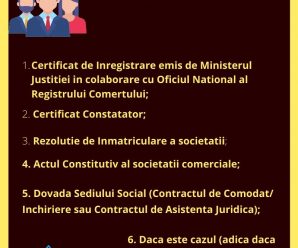
Infiintare firma: DOCUMENTE OFICIALE ALE UNEI SOCIETATII NOU INFIINTATE Certificat de Inregistrare emis de Ministerul Justitiei in colaborare cu Oficiul National al Registrului Comertului; Certificat Constatator emis in temeiul art. 17 indice 1 alin. 1 lit. (c) din Legea 359/
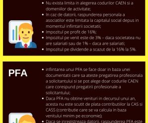
Infiintare firma: ce alegi SRL sau PFA? Infograficul de mai jos te ajuta sa vezi diferentele dintre cele doua tipuri de entitati juridice, astfel incat sa faci cea mai buna alegere cand vei demara afacerea ta. Infografic: Infiintare firma –

Infografic: Acte necesare infiintare SRL – Reinvent Consulting Acte infiintare SRL Registrul Comertului: Copie Carte de Identitate ( C.I.) sau Pasaport ale asociatilor si/sau administratorilor; Dovada rezervarea denumirii firmei; Dovada sediul social: contract de comodat, de inchiriere sau subinchiriere, de

Top 10 intrebari antreprenori Intrebare nr. 1: Daca am venituri din dividente, trebuie sa depun declaratia unica la ANAF? Intrebare nr. 2: Daca vreau sa inchid o firma suspendata la Registrul Comertului trebuie reactivata mai intai? Intrebare nr. 3: Pot infiinta un